- 您现在的位置:买卖IC网 > Sheet目录2006 > LTC2642IDD-16#PBF (Linear Technology)IC DAC 16BIT VOUT 10-DFN
LTC2641/LTC2642
14
26412fc
For more information www.linear.com/LTC2641
applicaTions inForMaTion
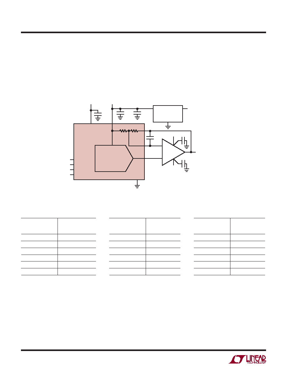
Bipolar Configuration
Figure 3 shows a typical bipolar DAC application for the
LTC2642. The on-chip bipolar offset/gain resistors, RFB
andRINV,areconnectedtoanexternalamplifiertoproduce
a bipolar output swing from –VREF to VREF at the RFB pin.
The amplifier circuit provides a gain of +2 from the VOUT
pin, and gain of –1 from VREF. Tables 2a, 2b and 2c show
the bipolar offset binary code tables for 16-bit, 14-bit and
12-bit operation.
–
+
16-BIT DAC
1/2 LT1678
5V
–5V
5V/3V
VREF
2.5V
VDD
LTC2642-16
BIPOLAR VOUT
–2.5V TO 2.5V
4.7F
C1
10pF
0.1F
REF
1
6
10
VOUT
7
INV
8
RFB
GND
26412 F02
0.1F
9
5
4
3
2
CS
SCLK
DIN
CLR
LT1019CS8-2.5
GND
OUT
5V
IN
Table 2b. 14-Bit Bipolar Offset Binary
Code Table (LTC2642-14)
DIGITAL INPUT
BINARY NUMBER
IN DAC LATCH
ANALOG OUTPUT
(VOUT)
MSB
LSB
1111 1111 1111 11xx VREF (8,191/8,192)
1000 0000 0000 01xx VREF (1/8,192)
1000 0000 0000 00xx 0V
0111 1111 1111 11xx –VREF (1/8,192)
0000 0000 0000 00xx –VREF
Figure 3. 16-Bit Bipolar Output (LTC2642-16) VOUT = –VREF to VREF
Table 2a. 16-Bit Bipolar Offset Binary
Code Table (LTC2642-16)
DIGITAL INPUT
BINARY NUMBER
IN DAC LATCH
ANALOG OUTPUT
(VOUT)
MSB
LSB
1111 1111 1111 1111 VREF (32,767/32,768)
1000 0000 0000 0001 VREF (1/32,768)
1000 0000 0000 0000 0V
0111 1111 1111 1111 –VREF (1/32,768)
0000 0000 0000 0000 –VREF
Table 2c. 12-Bit Bipolar Offset Binary
Code Table (LTC2642-12)
DIGITAL INPUT
BINARY NUMBER
IN DAC LATCH
ANALOG OUTPUT
(VOUT)
MSB
LSB
1111 1111 1111 xxxx VREF (2,047/2,048)
1000 0000 0001 xxxx VREF (1/2,048)
1000 0000 0000 xxxx 0V
0111 1111 1111 xxxx –VREF (1/2048)
0000 0000 0000 xxxx –VREF
发布紧急采购,3分钟左右您将得到回复。
相关PDF资料
LTC2704IGW-16#PBF
IC DAC 16BIT QUAD VOUT 44-SSOP
LTC2751AIUHF-16#PBF
IC DAC 16BIT CUR OUT 38-QFN
LTC2752ACLX#PBF
IC DAC 16BIT DUAL CUR OUT 48LQFP
LTC2753AIUK-16#TRPBF
IC DAC 16BIT DUAL 48-QFN
LTC2754AIUKG-16#PBF
IC DAC 16BIT QUAD IOUT 52-QFN
LTC2755AIUP-16#PBF
IC DAC 16BIT CUR OUT 64-QFN
LTC2757ACLX#PBF
IC DAC 18BIT PAR 48LQFP
LTC2758AILX#PBF
IC DAC 18BIT SPI/SRL 48-LQFP
相关代理商/技术参数
LTC2642IDD-16#TRPBF
功能描述:IC DAC 16BIT VOUT 10-DFN RoHS:是 类别:集成电路 (IC) >> 数据采集 - 数模转换器 系列:- 标准包装:47 系列:- 设置时间:2µs 位数:14 数据接口:并联 转换器数目:1 电压电源:单电源 功率耗散(最大):55µW 工作温度:-40°C ~ 85°C 安装类型:表面贴装 封装/外壳:28-SSOP(0.209",5.30mm 宽) 供应商设备封装:28-SSOP 包装:管件 输出数目和类型:1 电流,单极;1 电流,双极 采样率(每秒):*
LTC2642IMS-12#PBF
功能描述:IC DAC 12BIT VOUT 10-MSOP RoHS:是 类别:集成电路 (IC) >> 数据采集 - 数模转换器 系列:- 产品培训模块:LTC263x 12-, 10-, and 8-Bit VOUT DAC Family 特色产品:LTC2636 - Octal 12-/10-/8-Bit SPI VOUT DACs with 10ppm/°C Reference 标准包装:91 系列:- 设置时间:4µs 位数:10 数据接口:MICROWIRE?,串行,SPI? 转换器数目:8 电压电源:单电源 功率耗散(最大):2.7mW 工作温度:-40°C ~ 85°C 安装类型:表面贴装 封装/外壳:14-WFDFN 裸露焊盘 供应商设备封装:14-DFN-EP(4x3) 包装:管件 输出数目和类型:8 电压,单极 采样率(每秒):*
LTC2642IMS-12#TRPBF
功能描述:IC DAC 12BIT VOUT 10-MSOP RoHS:是 类别:集成电路 (IC) >> 数据采集 - 数模转换器 系列:- 产品培训模块:LTC263x 12-, 10-, and 8-Bit VOUT DAC Family 特色产品:LTC2636 - Octal 12-/10-/8-Bit SPI VOUT DACs with 10ppm/°C Reference 标准包装:91 系列:- 设置时间:4µs 位数:10 数据接口:MICROWIRE?,串行,SPI? 转换器数目:8 电压电源:单电源 功率耗散(最大):2.7mW 工作温度:-40°C ~ 85°C 安装类型:表面贴装 封装/外壳:14-WFDFN 裸露焊盘 供应商设备封装:14-DFN-EP(4x3) 包装:管件 输出数目和类型:8 电压,单极 采样率(每秒):*
LTC2642IMS-14#PBF
功能描述:IC DAC 14BIT VOUT 10-MSOP RoHS:是 类别:集成电路 (IC) >> 数据采集 - 数模转换器 系列:- 标准包装:47 系列:- 设置时间:2µs 位数:14 数据接口:并联 转换器数目:1 电压电源:单电源 功率耗散(最大):55µW 工作温度:-40°C ~ 85°C 安装类型:表面贴装 封装/外壳:28-SSOP(0.209",5.30mm 宽) 供应商设备封装:28-SSOP 包装:管件 输出数目和类型:1 电流,单极;1 电流,双极 采样率(每秒):*
LTC2642IMS-14#TRPBF
功能描述:IC DAC 14BIT VOUT 10-MSOP RoHS:是 类别:集成电路 (IC) >> 数据采集 - 数模转换器 系列:- 标准包装:47 系列:- 设置时间:2µs 位数:14 数据接口:并联 转换器数目:1 电压电源:单电源 功率耗散(最大):55µW 工作温度:-40°C ~ 85°C 安装类型:表面贴装 封装/外壳:28-SSOP(0.209",5.30mm 宽) 供应商设备封装:28-SSOP 包装:管件 输出数目和类型:1 电流,单极;1 电流,双极 采样率(每秒):*
LTC2642IMS-16#PBF
功能描述:IC DAC 16BIT VOUT 10-MSOP RoHS:是 类别:集成电路 (IC) >> 数据采集 - 数模转换器 系列:- 标准包装:1 系列:- 设置时间:4.5µs 位数:12 数据接口:串行,SPI? 转换器数目:1 电压电源:单电源 功率耗散(最大):- 工作温度:-40°C ~ 125°C 安装类型:表面贴装 封装/外壳:8-SOIC(0.154",3.90mm 宽) 供应商设备封装:8-SOICN 包装:剪切带 (CT) 输出数目和类型:1 电压,单极;1 电压,双极 采样率(每秒):* 其它名称:MCP4921T-E/SNCTMCP4921T-E/SNRCTMCP4921T-E/SNRCT-ND
LTC2642IMS-16#TRPBF
功能描述:IC DAC 16BIT VOUT 10-MSOP RoHS:是 类别:集成电路 (IC) >> 数据采集 - 数模转换器 系列:- 标准包装:47 系列:- 设置时间:2µs 位数:14 数据接口:并联 转换器数目:1 电压电源:单电源 功率耗散(最大):55µW 工作温度:-40°C ~ 85°C 安装类型:表面贴装 封装/外壳:28-SSOP(0.209",5.30mm 宽) 供应商设备封装:28-SSOP 包装:管件 输出数目和类型:1 电流,单极;1 电流,双极 采样率(每秒):*
LTC-2651TBE-01
制造商:LITEON 功能描述:8*4 ND, 0.28 inch, common anode, color-blue